
There is a wide range of materials used in the semiconductor industry.
You have ceramics, printed circuit boards, epoxy resins/molds, and silicon integrated circuits to name a few.
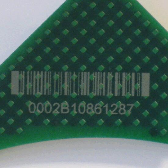
The big key when marking on semiconductor substrates is precision accuracy and depth control.
Accuracy is required to ensure proper placement and readability of markings that are commonly smaller than 1mm in size and read by vision systems.
Depth control limits the amount of particulate dust and thermal transfer to protect sensitive electronics or components.
ZGG 532nm Green laser marking systems are capable of meeting the standards of semiconductor marking applications.
The 532nm Green wavelength is inherently cooler than that of other lasers and provides less thermal transfer.
Along with the thermal benefits of the 532nm laser, increased absorption allows for less intense laser settings, which helps with precision depth control.
The 532nm lasers are capable of marking directly onto printed circuit boards without exposing the underlying copper layer.
These lasers can even mark silicon wafers or integrated circuits that can only be measured in angstroms.
Couple these inherent benefits with advanced optical control to create spot sizes as low as 10um, and you have the ideal laser for semiconductor applications.


